Inspiring Minds, Designing Chips

A Fabless Design & Training hub for Up-Skilling graduate engineers for the Semiconductor Industry and perform chip design research and development.

About us

NCDC is a national level initiative to ignite the semiconductor ecosystem in Pakistan. It aims to be an inclusive, open and collaborative entity with a vision to facilitate universities, industries and engineering graduates, thereby placing Pakistan on the global semiconductor map. Key features include

  • Train-to-Hire Chip Design & Manufacturing Trainings
  • University Memberships & Industrial Partnerships
  • EDA Tools, PDKs, and Tape-outs
  • Chip Design Startup Incubation
  • Chip Testing Services
  • Cutting-edge R&D and much more…

Trainings

  • Industry Validated Curriculum & Expert Trainers
  • Hands-on experience using industry-standard EDA tools
  • Complete design to tape-out cycle
  • Manufacturing and OSAT training
  • Incubation possibilities at training completion
  • Stipends available
  • Soft-skills mentoring & Extra-curricular activities
  • Exit interviews of successful trainees by chip design companies

Digital IC Design

  • Computer Architecture
  • RISC-V
  • Advanced Digital Design
  • C Programming
  • RTL to GDS Flow using Cadence & Open Source Tools
  • FPGA Prototyping

Analog & Mixed Signals IC Design

  • MOS Device to Circuit understanding
  • Analog design cycle including schematic & layout
  • Practical circuit design experience of OTAs, BGR, LDO, VCO, PLL and data converters
  • DRC, LVS & chip sign-off process

Digital Design Verification

  • Computer Architecture
  • RISC-V
  • C Programming
  • SystemVerilog
  • System Verification using UVM
  • Fundamentals of Linux & Git 

Semiconductor Manufacturing

  • Manufacturers Overview
  • Semiconductor lifecycle, supply chain & fab processes
  • Test & Product Engineering to manage Fabless products
  • Quality & Reliability for die & package qualification
  • IC Failure analysis, QMS process and flows

PCB & Package Design

  • Multi-layer, Mixed Signal PCB Design
  • DFM & DFT considerations
  • Signal, Power Integrity, EMC, Thermal Analysis
  • Design for Manufacturing, Assembly, Testing
  • Advanced Package Design, Heterogeneous Integration

Our Team

Project Director

Dr Hammad M Cheema

Analog & RF IC Design

Deputy Project Director

Dr. Waqar Ahmed

Digital IC Design

IC Designers

Karam Ellahi

Analog & Mixed Signal IC Design

Muhammad Haris Farooq

Analog & Mixed Signal IC Design

Shirin Qaisar

Analog & Mixed Signal IC Design

Syed Muhammad Sarmad

Digital IC Design

Muhammad Bilal

Digital IC Design

Hira Sohail

Digital IC Design

Chip Gallery

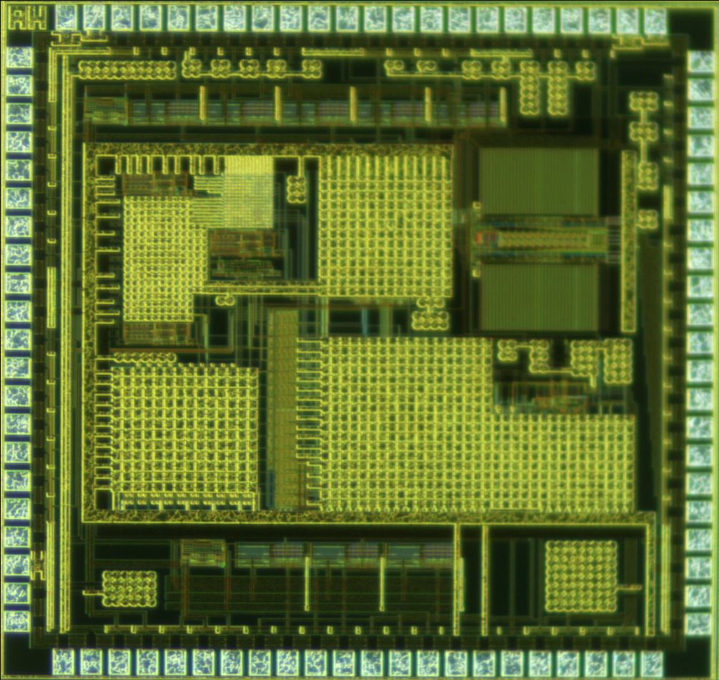
Electro-Impedance Tomography Measurement IC

(2 x 1.9 mm.sq)

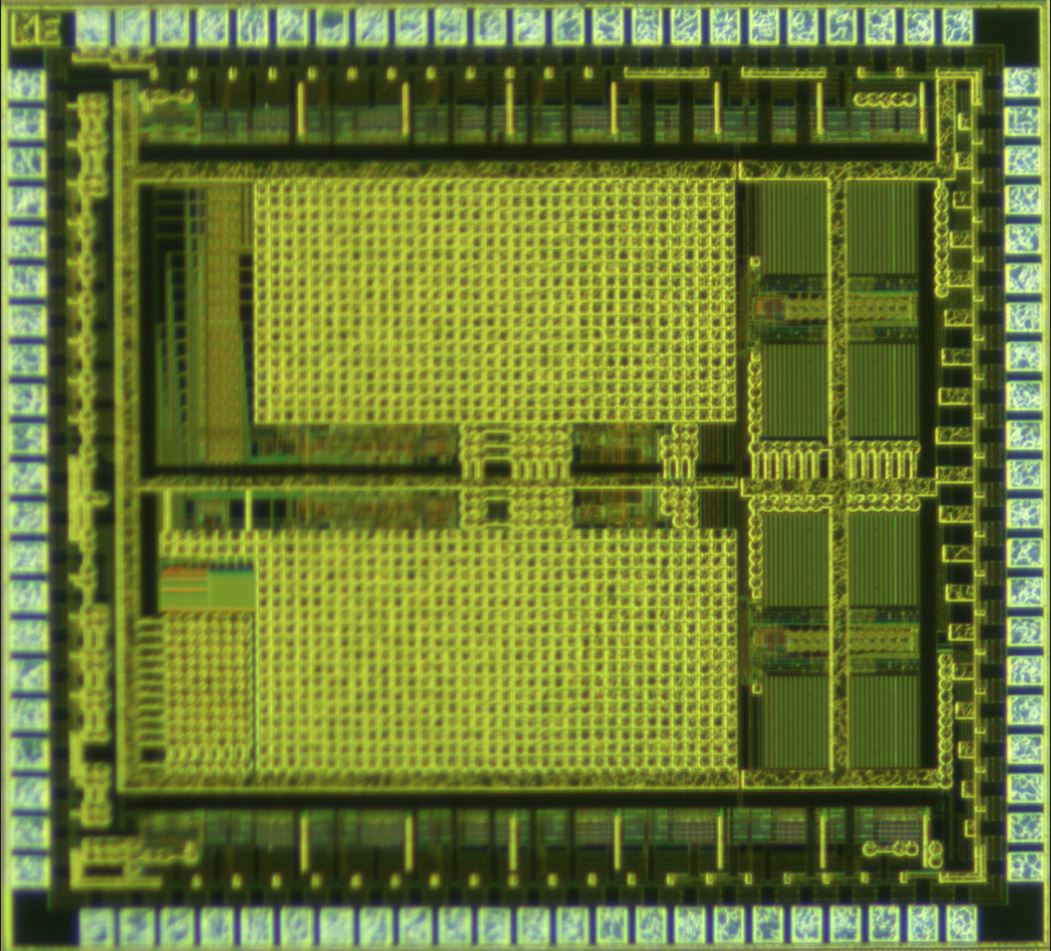
High-Throughput Impedance-Measurement IC

(2.1 x 1.9 mm.sq)

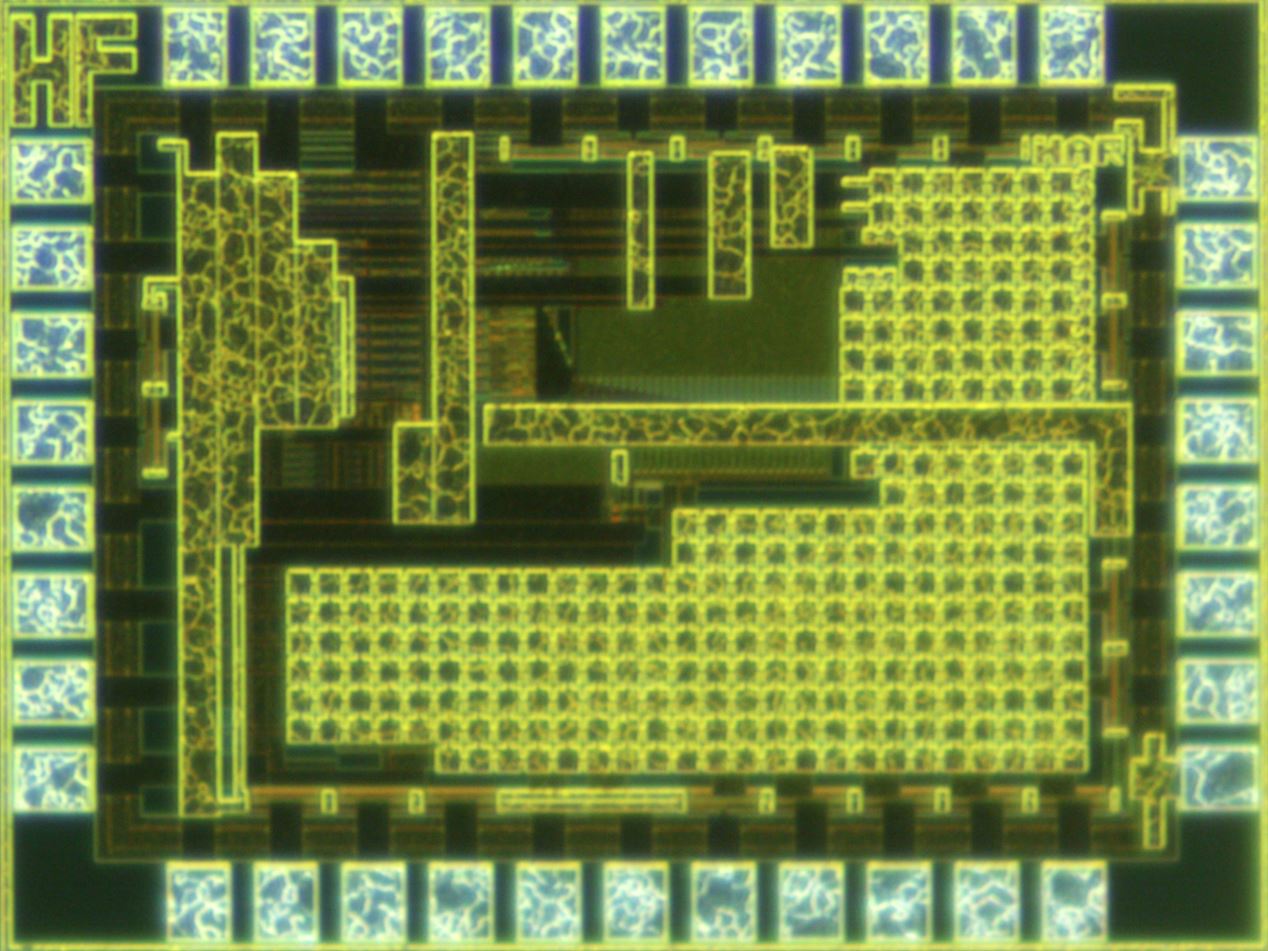
Analog Assisted Digital Low Dropout Regulator (LDO) Chipset

(1.1 x 0.8 mm.sq)

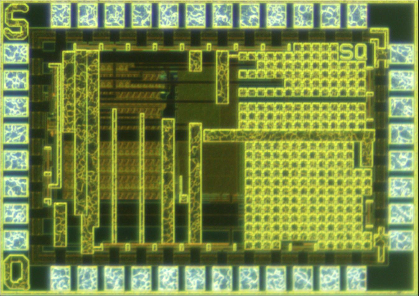
Tri-Loop Low Dropout Regulator (LDO) for Power Management in SoCs

(1.2 x 0.8 mm.sq)

Activities

Our Collaborators

Contact Information

Location: NUST Chip Design Centre (NCDC), National University of Sciences & Technology
SINES building, Sector H-12, Islamabad.

Phone Number: 03028641252

Email: contact@ncdc.nust.edu.pk